Pinout for development port is confusing.

Hi there,
I’m a little confuse regarding the I2C ports on the development port.
Base on this image


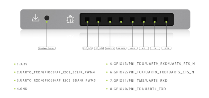
I understand that the pin number 1 is on the far right (3.3v) and the pin number 8 is on the far left.
The pins 7 and 8 (GPIO71 and GPIO70 respectively ) are use as I2C_SDA anf I2C_SCL.
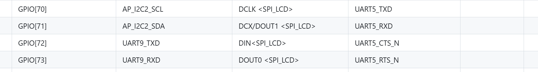
However, that text on the bottom right corner says that pins GPIO70 and GPIO71 are use as follow:

7 - GPIO71/PRI_TMS/UART5_RXD
8 - GPIO70/PRI_TDI/UART5_TXD

There is no I2C mention there. Base on the text, I would believe that the port use as I2C are the number 2 and 3 (GPIO68 and GPIO69)

I’m confused here.
Could someone make it clear?

Thanks.

sorry , this images is wrong about I2C bus. we will update this images, and “I2C2” was used by GPIO84,GPIO85 on motherboard, if other GPIO use I2C2, the EEPROM, AUDIO will loss signal.
So I2C ports will be remove on the development port.

So is not possible to use an I2C with the development port at all or just use GPIO68 and GPIO69?
Thanks for the reply.

It is not possible to use an I2C with the development port at all


What else is connected to AP_I2C2_SCL, AP_I2C2_SDA?
What if I don’t use or need what ever is connected to that I2C?
What we can really use for the debug port?

Thanks